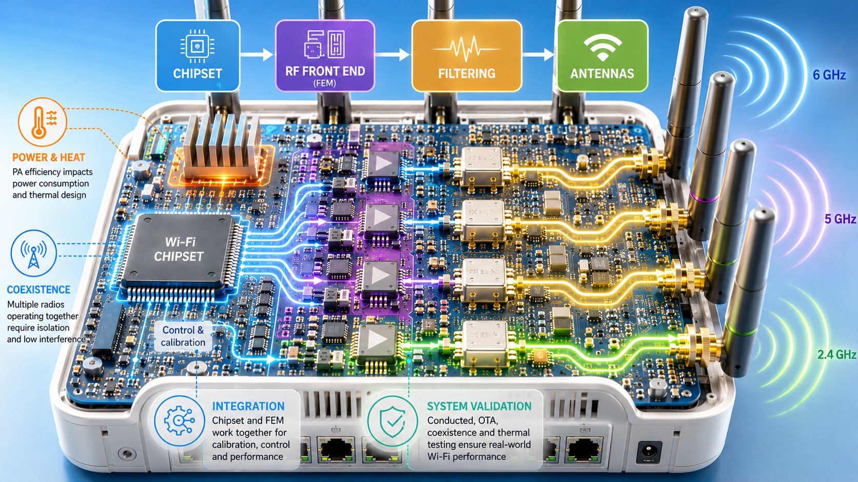

A high-performance Wi-Fi chipset does not guarantee a high-performance Wi-Fi device. Neither does a powerful FEM, a low-loss filter, or a well-designed antenna. What ultimately determines RF performance is how all of these elements work together as a system. That system is becoming considerably harder to design.
Wi-Fi APs and other devices increasingly need to support many frequency bands, multiple spatial streams, wide channels, high-order modulation, simultaneous transmissions, Bluetooth and sometimes cellular radios – all within tight constraints on size, cost and power consumption. At the same time, the RF chain needs to preserve extremely demanding signal quality from the Wi-Fi chipset all the way to the antenna. This makes RF front-end integration one of the less visible – but increasingly important – challenges in Wi-Fi equipment design.
From chipset to antenna: One RF system
It is tempting to think of the Wi-Fi radio as a chain of relatively independent components: Wi-Fi chipset → FEM → filters → antenna In practice, the boundaries are much less clear. The output characteristics of the Wi-Fi chipset affect what the power amplifier must handle. The PA affects linearity, power consumption and heat generation. Filters introduce insertion loss while providing the isolation required between radios and frequency bands. PCB traces, connectors and switches introduce additional losses. Antenna efficiency and placement ultimately determine how much of the available RF energy becomes useful radiated power.
Changing one part of the chain can therefore affect several others. For equipment designers, the relevant question is rarely simply “Which FEM has the highest output power?” It is closer to: Which combination of chipset, FEM, filtering, board design and antennas delivers the required Wi-Fi performance within our power, thermal, size and cost constraints? That is a much harder optimization problem.
More radios mean more integration challenges
The RF problem becomes more difficult as Wi-Fi devices add bands and spatial streams. A tri-band access point supporting 2.4 GHz, 5 GHz, and 6 GHz may contain several RF chains for each band. Multi-Link Operation (MLO) can also mean that multiple Wi-Fi links are active at the same time. The result is a dense RF environment inside the device itself.
Transmitters can interfere with receivers. Harmonics and other unwanted emissions need to be controlled. Signals need sufficient isolation between bands and RF chains. Antennas need to be positioned so that they interact as little as possible, while still fitting within the physical constraints of the product. This is where FEM and filter specifications alone stop telling the whole story.
A filter may offer excellent selectivity but introduce additional insertion loss. Better antenna isolation may require more physical separation than the enclosure allows. Higher PA output power may improve link budget but increase heat generation and make linearity more difficult to maintain. RF design consequently becomes a series of system-level trade-offs.
FEM and chipset integration is becoming more important
The relationship between the Wi-Fi chipset and the FEM is also changing. Traditionally, much of the RF front end could be treated as a relatively independent analog subsystem. Increasingly sophisticated techniques can require much tighter interaction between the chipset and the FEM.
Digital pre-distortion (DPD) – as discussed in Part 3 of this series – is an important example. DPD attempts to compensate for the nonlinear behaviour of the power amplifier by deliberately modifying the signal before amplification. For this to work effectively, the system needs an accurate understanding of the PA’s behaviour and a mechanism for applying the appropriate correction.
In Wi-Fi implementations, this can require participation from the Wi-Fi chipset vendor as well as the FEM supplier. Digital control, calibration, characterisation, and software integration may all become part of bringing the RF chain into production. The engineering challenge is therefore not limited to designing a better PA. The chipset and front end increasingly have to be designed – or at least validated – to work together.
This has commercial consequences as well as technical ones. Integration work costs money, consumes engineering resources and can lengthen product development cycles. It also helps explain the interest in alternative approaches to PA linearisation. Architectures such as the approach being developed by QuantalRF – discussed in Part 3 – seek to improve PA linearity without relying on conventional chipset-controlled DPD. If such approaches can achieve the required RF performance, one potential system-level advantage is reducing some of the chipset/FEM interworking and integration associated with DPD.
The important question is therefore not only which architecture produces the best laboratory RF measurements, but which architecture produces the required performance with acceptable system complexity.
Filters have to be evaluated as part of the RF chain
Filters present a similar optimization problem. The ideal filter would completely reject every unwanted frequency while allowing the desired signal to pass without loss. Real filters cannot do this. Greater selectivity, lower insertion loss, higher power handling, small physical size and low cost can pull the design in different directions. Insertion loss is particularly important because every fraction of a decibel lost between the PA and antenna reduces effective transmit performance. Loss in the receive path also reduces sensitivity.
This means that filtering cannot simply be maximised. The objective is to provide enough isolation and rejection to allow the radios to coexist while minimising the RF penalty imposed on the wanted signal. As discussed in Part 2, this becomes particularly challenging around the boundaries between Wi-Fi spectrum and neighbouring services. But the final result depends not only on the filter itself. Antenna isolation, PCB layout, shielding and the radio architecture all contribute to the overall coexistence performance.
PCB layout can consume the RF budget
At Wi-Fi frequencies, the circuit board itself is part of the RF system. RF signals travelling between the chipset, FEM, filters and antennas experience losses. Transmission-line geometry, impedance matching, component placement, vias, connectors, and routing all matter. At 5 GHz and 6 GHz in particular, apparently small layout decisions can have measurable consequences.
This creates another important distinction between component-level and product-level performance. A FEM may produce a particular output power under controlled test conditions. The power reaching the antenna in an actual access point can be lower after switches, filters, PCB traces and other losses are included. The same principle applies on receive. The complete RF path therefore needs to be optimized – not merely the individual components.
Heat is part of RF design
Thermal design is also inseparable from RF design. As discussed in Part 1, power amplifiers convert only part of the electrical power they consume into useful RF energy. The remainder largely becomes heat. More RF chains mean more potential heat sources. Simultaneous operation can make the problem worse.
Equipment vendors then need to remove that heat through PCB design, heat spreaders, heatsinks, airflow, or other thermal mechanisms. These measures consume physical space and add cost. Temperature can also affect RF component behaviour and ultimately the performance that can be sustained under load.
This is why PA efficiency matters beyond electricity consumption. Every improvement in RF efficiency can potentially reduce the thermal burden elsewhere in the product. Conversely, achieving a small increase in RF output power at the cost of significantly greater DC power consumption may be a poor system-level trade.
The antenna completes the RF chain
The antenna is the final stage between the RF electronics and the real world. A powerful transmitter feeding an inefficient or poorly positioned antenna will not deliver the expected coverage. Similarly, a well-designed receive chain cannot recover signal energy that the antenna fails to capture.
Antenna placement becomes particularly challenging in compact multi-radio products. Multiple antennas must support MIMO while providing suitable spatial and polarisation characteristics. They may also need sufficient isolation to allow simultaneous operation across different radios and bands. Mechanical design therefore becomes part of RF design. Enclosure materials, antenna placement, PCB orientation and even nearby components can influence the final radiation characteristics. This is another reason why conducted RF measurements alone cannot describe the performance of the finished Wi-Fi product.
Validation must move beyond individual components
Component specifications remain essential, but the final RF system needs to be validated under realistic operating conditions. That can include conducted measurements of transmit power, EVM and receiver sensitivity, but also over-the-air testing, thermal testing and coexistence testing. Increasingly, it also means testing combinations of conditions.
What happens when multiple Wi-Fi radios transmit simultaneously? What happens when the device becomes hot? Does EVM remain within specification at high output power? Does a transmitter in one band desensitise a receiver operating in another? These are system questions. And as Wi-Fi equipment becomes more complex, they become increasingly important to answering the question that ultimately matters: Does the finished device deliver the expected Wi-Fi performance in the conditions in which customers will actually use it?
Integration complexity has an economic implications
The RF front end is therefore not only an engineering problem – it is also an economic one. More complex architectures can require additional components, calibration, software development, validation, and cooperation between suppliers. They can increase PCB area, thermal requirements and development time. Equipment vendors consequently have to evaluate RF solutions against more than headline specifications. Relevant metrics increasingly include:
- RF performance: Output power, EVM, sensitivity and coexistence performance.
- Power efficiency: How much electrical power is required to achieve the target RF performance.
- Thermal impact: How much heat must be managed inside the product.
- Integration effort: How difficult the RF solution is to integrate with the selected Wi-Fi platform.
- Calibration requirements: What needs to happen during manufacturing and throughout operation.
- PCB requirements: Space, routing complexity and external components.
- Cost: Both component cost and the broader cost of implementing the architecture.
- Time to market: How much engineering and validation are required before the product can ship.
The FEM with the best individual specification is therefore not necessarily the FEM that produces the best Wi-Fi product.
WiFi NOW’s take: The Wi-Fi RF front end should increasingly be viewed as a system rather than a collection of components. Chipsets, power amplifiers, filters, switches, PCB design, antennas, thermal management and software all contribute to the final result—and improving one element can create costs or compromises somewhere else. This is particularly important as the industry explores more sophisticated approaches to PA linearity and efficiency. Conventional DPD can deliver important benefits, but it can also create tighter dependencies between Wi-Fi chipsets and FEMs. Alternative architectures may offer different trade-offs.
For equipment makers, the winning RF solution will therefore not necessarily be the one with the highest output power, the sharpest filter or the most sophisticated linearisation technology. It will be the architecture that delivers the required Wi-Fi performance with the best combination of power efficiency, RF quality, integration complexity, thermal performance and cost. And that system-level optimization is likely to become even more important as Wi-Fi moves into its next generation.